Intel Shows Off 8-core, 528-thread Processor With 1TB/s Of Co-packaged Optics

Hot Chips Intel has used this week’s Hot Chips conference in California to show off a 528-thread processor with 1TB/s silicon photonics interconnects that's designed to chew the largest analytics workloads, while sipping power.
For those hoping for a hyper-parallelized Xeon, this isn't that. The chip isn't even x86 based.
Instead, it was purpose built using a custom RISC architecture for DARPA's Hierarchical Identity Verify Exploit (HIVE) program. That US military initiative seeks to develop a graph analytics processor capable of churning through streaming data 100 times faster than conventional compute architectures, while also consuming less power.
Graph analytics deal with how data points connect with other data points in complex systems. The example Intel principal engineer Jason Howard pointed to in his Hot Chips presentation was social networks, which might run graph analytics workloads to understand connections among members.
Think of it as a really high-performance Six Degrees of Separation (or Kevin Bacon) and you’ll get the idea.
While this might seem a strange thing for DARPA to consider, the government agency feels large scale graph analytics has applications in infrastructure monitoring and cybersecurity.
The chip is part of Intel's first direct mesh-to-mesh photonic fabric, which uses silicon photonic interconnects to stitch multiple chips together. But rather than using copper to stitch two, four or even eight sockets together using copper traces, Intel used co-packaged optics to connect hundreds or even thousands of chips together in a low latency, high bandwidth mesh.
That's the idea anyway, the chip is still a prototype.
Scaling up graph analytics with silicon photonics
The goal is to develop tech that can be scaled up to support even the largest graph analytics workloads.

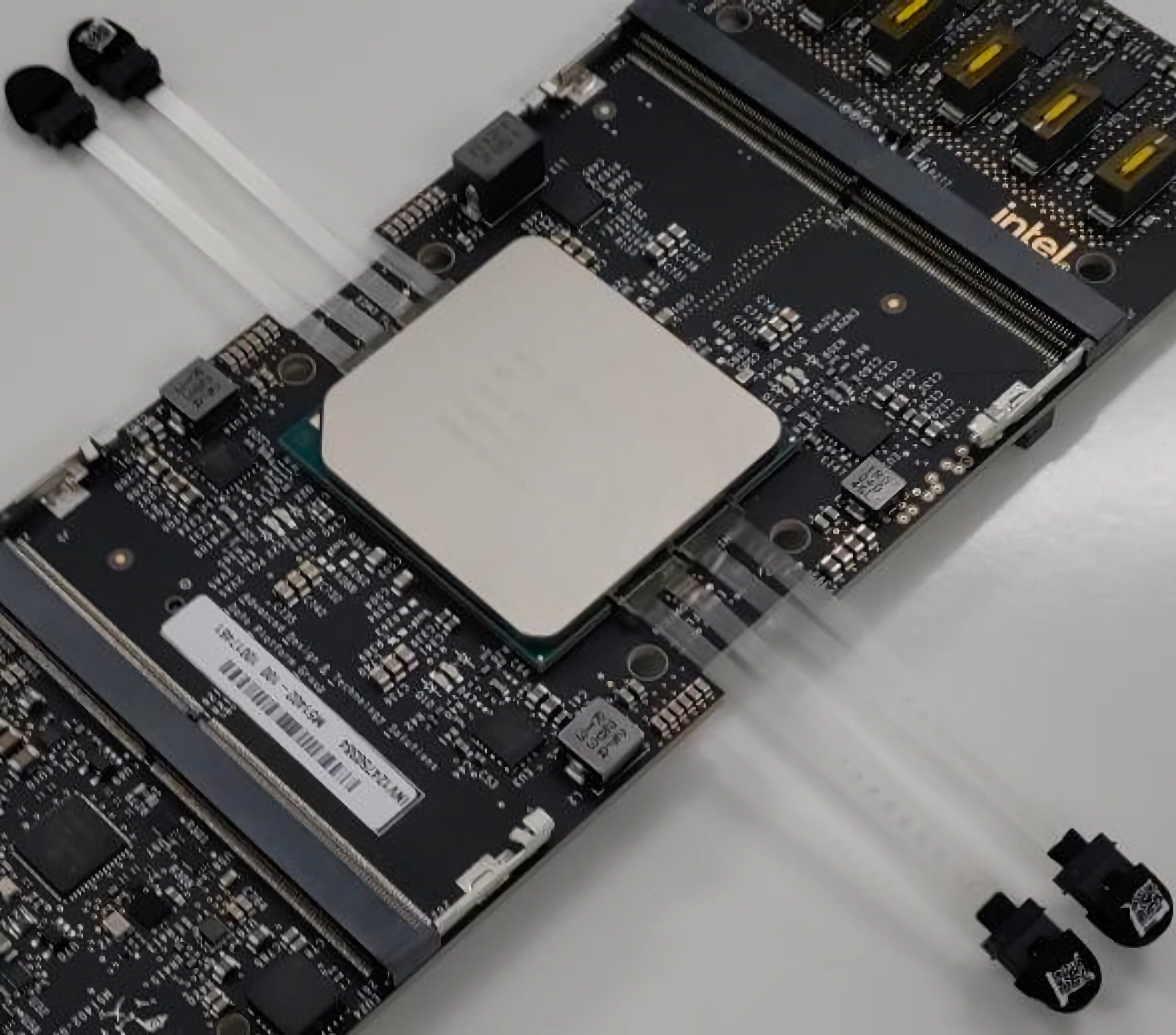
The four chiplets surrounding the central compute die supply the Intel prototype with 1TB/s of optical bandwidth - Click to enlarge
While the chip initially appears to be a standard processor with some extra bits and bobs — it even has a fairly typical BGA interface not unlike those found on Xeon-D chips — most of the data flowing in and out of the chip is transmitted optically using silicon photonics chiplets developed in collaboration with Ayar Labs.
The four little chiplets surrounding the central processing die convert the electrical signals coming in and out of the microprocessor to optical signals carried by 32 single-mode fibers. As we understand it 16 of those fiber strands are for transmitting data and the other 16 are for receiving it.
According to Intel, each of those fibers can carry data at 32GB/s on and off the chip for an aggregate of 1TB/s of bandwidth. However, Howard said that in testing the team had only managed to achieve half that rate.
As Intel envisions it, 16 of these chips would be networked together in an all-to-all configuration on a single Open Compute Project server in its sled form factor. Then multiple sleds, potentially as many as 100,000, could be networked together again in a sled-to-sled configuration. The result would be that any one chip could communicate with another, at very low latencies, regardless of which sled it resides in.
That's not to say the x86 goliath didn't run into challenges getting the optics to cooperate. In addition to only achieving half the bandwidth as advertised, Howard said fibers often misbehaved or broke.
"Once we got everything aligned and working, there were a lot of fiber attachment issues where they would just pop off because these are brittle fibers," Howard said. "We also saw, when we were doing the reflow process of the overall package, that we would run into optical problems due to thermal results, and we would end up having bad optical yields."
To overcome these challenges Intel had to work with its partners to develop new materials with lower thermal barriers, Howard explained.
- AMD on the edge: Stripped down Siena Epycs teased
- Google sharpens AI toolset with new chips, GPUs, more at Cloud Next
- Intel promises next year's Xeons will challenge AMD on memory, IO channels
- Arm reveals just how vulnerable it is to trade war with China
Tackling silicon bottlenecks
This novel system was needed because while Intel’s current commercial kit speeds through graph analytics workloads, it struggles to scale.
"A Xeon can pretty much take one of the graph datasets and store it in its cache and just churn through it really quickly," said Intel’s Howard. However, when you start to scale those datasets you start running into performance and efficiency bottlenecks.
So, the team set out to develop a new kind of processor optimized for graph analytics and quickly discovered several quirks inherent to the workload that could be optimized for in silicon.
"We immediately saw that they are massively parallel, in fact, embarrassingly parallel, so we could exploit a lot of parallelism to improve the overall performance," Howard said, adding that the team also uncovered issues with memory and cache utilization.
"When we would bring a cache line into the processor, we would only usually use eight bytes of it and then end up throwing away the other 64 bytes without ever utilizing them," he said, explaining that this put unnecessary strain on the system any time there were a bunch of big out of order pipelines.

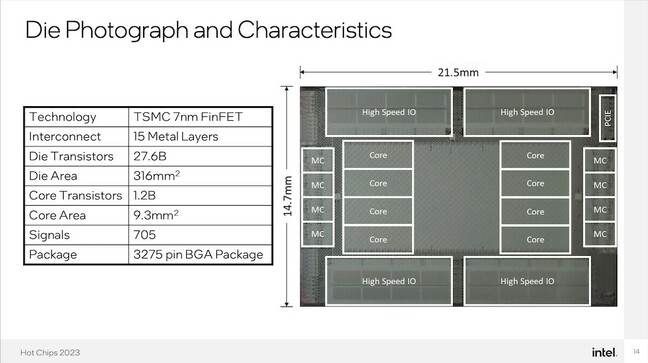
A significant chunk in the center of the die is dedicated to routers which control the flow of data streaming in from the co-packaged optics. - Click to enlarge
These design considerations drove the team to develop this experimental processor, which TSMC builds using its 7nm FinFET process (in case you didn't know, Intel fabs a lot of non-CPU products at TSMC and has for years) and which features eight cores each with 66 threads.
The chip also uses a novel memory architecture, an important inclusion to optimize it for graph analytics workloads, Howard explained. The chips are paired with 32GB of DDR5 4400MT/s memory which was accessed through a custom memory controller that allowed for 8-byte access granularity. According to Howard, this was advantageous as "anytime we're pulling a data line out of memory, we're going to try to utilize all of that data line as opposed to throwing away 7/8ths of it."
PCIe 4.0 with an 8x connection allows for connectivity back to the host system.
Intel also had to figure out a way to deal with the sheer volume of traffic coming in and out of the compute die, which in theory could be as much as 1TB/s. According to Howard, that requirement is the reason plenty of the die is dedicated to routers.
And while you might think such a thread and network heavy chip might run hot, it doesn't. The chip tops out at 75 watts at 1GHz. According to Intel, a 16-sled configuration would handle 8TB of memory, 2,048 cores, 135,168 threads, and consume roughly 1.2kW of power. That's not bad considering that a single dual-socket Sapphire Rapids system with 112 cores and 224 threads could easily consume that much power under load.
Intel imagines these chips could be built into rigs that scale to meshes encompassing 100,000 sleds and achieve near linear performance scaling for even the largest graph analytics workloads. However, this dream remains just that, as Intel has so far tested just two chips connected on its fabric.
Whether Intel ever commercializes the design is going to depend on funding, Howard explained. "If people want to give us money, we are more than welcome to build these things out." ®
From Chip War To Cloud War: The Next Frontier In Global Tech Competition
The global chip war, characterized by intense competition among nations and corporations for supremacy in semiconductor ... Read more
The High Stakes Of Tech Regulation: Security Risks And Market Dynamics
The influence of tech giants in the global economy continues to grow, raising crucial questions about how to balance sec... Read more
The Tyranny Of Instagram Interiors: Why It's Time To Break Free From Algorithm-Driven Aesthetics
Instagram has become a dominant force in shaping interior design trends, offering a seemingly endless stream of inspirat... Read more
The Data Crunch In AI: Strategies For Sustainability
Exploring solutions to the imminent exhaustion of internet data for AI training.As the artificial intelligence (AI) indu... Read more
Google Abandons Four-Year Effort To Remove Cookies From Chrome Browser
After four years of dedicated effort, Google has decided to abandon its plan to remove third-party cookies from its Chro... Read more
LinkedIn Embraces AI And Gamification To Drive User Engagement And Revenue
In an effort to tackle slowing revenue growth and enhance user engagement, LinkedIn is turning to artificial intelligenc... Read more

