Nvidia's Accelerated Cadence Spells Trouble For AMD And Intel's AI Aspirations

Analysis In the mad dash to capitalize on the potential of generative AI, Nvidia has remained the clear winner, more than doubling its year-over-year revenues in Q2 alone. To secure that lead, the GPU giant apparently intends to speed up the development of new accelerators.
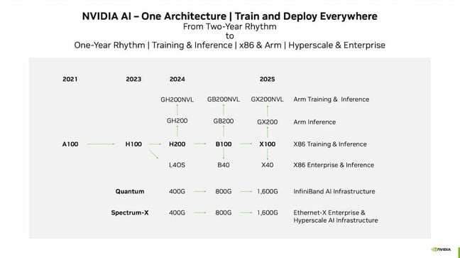
For the past few generations, a two-year cadence was enough to retain a competitive edge. But according to slides [PDF] from an investor presentation earlier this month, we'll not just see the B100 but a new "Super Chip" pairing Arm cores with the Blackwell architecture as well as a replacement for the L40 and L40S.
No real surprises there, we'd all expected to hear about Nvidia's next-gen architecture and the B100 in its various forms sometime in 2024.
It's what comes next that's surprising.

According to an investor presentation released this month, Nvidia plans to shift from a two-year to a one-year release cadence (click to enlarge)
The slides suggest that Nvidia will be moving to a one-year release cadence. On the slide, we see that the Blackwell-based B100 and its contemporaries will be superseded in 2025 by an "X100" class of parts. We assume "X" here is a placeholder while Huang mulls which mathematician, computer scientist, or engineer to dedicate the architecture to. But the point remains: Nvidia intends to roll out new GPUs faster than ever.
What does this mean for Intel and AMD?
The shift poses a potential problem for vendors like AMD and Intel which are still on a two-year release cadence for GPUs and AI accelerators.
AMD, for instance, introduced its Instinct MI200-series accelerators about a year after Nvidia's A100, claiming substantially better double-precision performance and comparable FP16 FLOPS, so long as you ignored Nvidia's support for sparsity.
The former gave the company a clear advantage in high performance computing applications compared to the A100, so it's no surprise that it has become such a popular part in supercomputers like Europe's Lumi or the Department of Energy's Frontier Supercomputers.
Now with generative AI drumming the demand beat, AMD hopes to challenge Nvidia's dominance in the AI arena with GPUs and APUs better tuned for lower precision workloads. But, if the performance estimates for the MI300A/X that our sibling site The Next Platform has put together are anything to go by, AMD's latest chips may not end up being competitive with the H100 on FLOPS, but could have an advantage in terms of memory. The chips are slated to offer 128GB-192GB of HBM3 memory, which could give the chips a narrow edge over the H100.
Intel, which made a big deal about AI at its Innovation conference in September, is in a similar boat. The company had already embraced an accelerated release cadence for CPUs and GPUs, but backed out of the latter amid a restructuring of the division and cost-cutting measures.
This decision resulted in the cancellation of both its XPU CPU-GPU architecture and Rialto Bridge, the successor to the Ponte Vecchio accelerators that power Argonne National Lab's Aurora supercomputer. The company then delayed its redefined Falcon Shores design from 2024 until 2025, arguing that the move "matches customer expectations on new product introductions and allows time to develop their ecosystems."
The latter is interesting, as it will see Intel bring its GPU Max and Habana Labs architectures under a single platform. Until then, we're stuck with Intel's Gaudi2 and GPU Max families until Gaudi3 ships.
Gaudi2 demonstrated respectable performance compared to the A100, but, by the time it launched last year, Nvidia's more capable H100 had already been announced and was months away from shipping.
Habana's next-gen accelerator, Gaudi3, looks promising, but it won't just have to outperform the H100 and AMD's MI300-series parts, but contend with the impending launch of Nvidia's B100 accelerators as well.
This doesn't mean that either MI300 or Gaudi3 are necessarily going to be dead on arrival, rather their window of relevance could end up being much shorter than in the past, SemiAnalysis founder Dylan Patel, who was among the first to pick up on the accelerated roadmap, told The Register.
"There is a window where MI300 is the best chip on the market," he said, adding that while we don't know nearly as much about Intel's Gaudi3, if it scales the way he expects, it'll be better than Nvidia's H100.
Long term, he expects Intel and AMD will have to follow suit and accelerate their own GPU and accelerator development roadmaps.
And as we've pointed out in the past, even if Intel and AMD's next-gen accelerators can't beat Nvidia, they may end up scoring wins based solely on availability. Nvidia's H100s are reportedly being constrained by the availability of advanced packaging tech provided by TSMC. This shortage isn't expected to clear up until 2024. And while AMD is likely to run into similar challenges with its MI300-series parts, which also utilize these advanced packing techniques, Intel has the capacity to do its own packaging, though it's not clear whether Gaudi3 actually uses it, or if they're in the same boat as Nvidia and AMD.
Not just about the accelerators
But it's worth noting that Nvidia isn't just accelerating the release cadence of its accelerators. It's also speeding up development of its Quantum Infiniband and Spectrum Ethernet switching portfolios.
While a single GPU alone is capable, AI training and HPC applications usually require large clusters of accelerators to operate efficiently and that means having networking capable of keeping up with them.
With the acquisition of long-time partner Mellanox in 2020, Nvidia took control over its network stack, which includes the company's switching and NIC portfolios.
For the moment Nvidia's fastest switches top out at 25.6Tbps for Infiniband and 51.2Tbps for Ethernet. That bandwidth is divided up amongst a bunch of 200-400Gbps ports. However, under this new release cadence, Nvidia aims to push port speeds to 800Gbps in 2024 and 1,600Gbps in 2025.
This will not only necessitate more capable switch silicon in the range of 51.2-102.4Tbps of capacity but faster 200Gbps serializer/deserializers (SerDes) to support 1,600Gbps QSFP-DD modules.
The technology required to achieve this level of network performance already exists. 200Gbps SerDes have already been demoed by Broadcom. However, we've yet to see it from Nvidia just yet. And ideally, Patel notes, Nvidia is going to want to get to 102.4Tbps on both Infiniband and Ethernet to really capitalize on 800Gbps capable NICs.
- Intel slaps forehead, says I got it: AI PCs. Sell them AI PCs
- Beijing-backed server chip startup formed by ex-Arm China execs
- Latest SiFive RISC-V cores aim to boost performance, accelerate AI workloads
- AI processing could consume 'as much electricity as Ireland'
A PCIe problem
This is where the cracks in Nvidia's master plan could begin to show. These higher speeds may not be tenable on such a timeline using existing NICs due to PCIe limitations. Today, the practical limit for a NIC is a single 400Gbps port. PCIe 6.0 should get us to 800Gbps, but we'll need PCIe 7.0 before we can talk seriously about 1,600 Gbps.
We already know that Intel's next-gen Xeons won't support PCIe 6.0 when they launch in 2024, and we just don't know enough about AMD's upcoming Turin Epycs to say whether they will or not. Though AMD has, over the past few generations, led Intel on the roll out of new PCIe standards.
However, x86 isn't Nvidia's only choice. The company has its own Arm-based CPUs now. So perhaps Nvidia plans to support PCIe 6.0 on the successor to Grace. Arm processors were among the first to add support for PCIe 5.0 in early 2022, so there's reason to believe that could happen again.
Because of this problem, Patel expects there to actually be two versions of the B100. One that uses PCIe 5.0 and has the same 700 watt thermal design power (TDP) as the H100, so customers can slot in a new HGX motherboard into their existing chassis designs. The second, he reckons, will be much higher power, require liquid cooling, and make the switch to PCIe 6.0.
However, when you start talking about 1,600 Gbps ports like Nvidia wants to jump to in 2025, you're going to need PCIe 7.0, which hasn't been finalized. "You talk to the standards body, nobody expects anything PCIe 7.0 until 2026 at the earliest for products," he said. "It's just impossible to do on that timeline."
The other option is to bypass the PCIe bus. As Patel points out, Nvidia doesn't actually need PCIe 6.0 or PCIe 7.0 levels of bandwidth between the GPU and CPU, just between the NIC and GPU. So instead, he expects Nvidia will largely bypass the CPU as a bottleneck.
In fact, Nvidia is already doing this to a degree. In more recent generations, Nvidia has effectively daisy chained the GPUs off their ConnectX NICs by using a PCIe switch. Patel says Nvidia is likely to expand on this approach to achieve port speeds higher than a single PCIe 5.0 or PCIe 6.0 x16 slot would otherwise be able to accommodate.
And with the X100-generation, he says there are rumors that Nvidia may ditch PCIe for communications between the NIC and GPU for X100 in 2025 in favor of their proprietary interconnect.
Speaking of which, those who have been paying attention to Nvidia's AI developments may be wondering where the chipmaker's super-high-bandwidth NVLinks fabric fits in. The tech is used to mesh together multiple GPUs so that they effectively behave as one large one. Add in an NVLink switch, and you can extend to multiple nodes.
However, there are some significant limitations to NVLink, particularly when it comes to reach and scalability. While NVLink is much faster than either, it's also limited to 256 devices. To scale beyond this, you'll need to employ Infiniband or Ethernet to stitch together additional clusters.
The NVLink mesh is also only good for GPU-to-GPU communications. It won't help with getting data in and out of the system or coordinating workloads.
As a result, whether or not Nvidia is successful in speeding up its release schedule is going to depend heavily on getting the networking to ramp fast enough to avoid choking its chips. ®
Need more? Check out The Next Platform's take on Nvidia's blueprint.
From Chip War To Cloud War: The Next Frontier In Global Tech Competition
The global chip war, characterized by intense competition among nations and corporations for supremacy in semiconductor ... Read more
The High Stakes Of Tech Regulation: Security Risks And Market Dynamics
The influence of tech giants in the global economy continues to grow, raising crucial questions about how to balance sec... Read more
The Tyranny Of Instagram Interiors: Why It's Time To Break Free From Algorithm-Driven Aesthetics
Instagram has become a dominant force in shaping interior design trends, offering a seemingly endless stream of inspirat... Read more
The Data Crunch In AI: Strategies For Sustainability
Exploring solutions to the imminent exhaustion of internet data for AI training.As the artificial intelligence (AI) indu... Read more
Google Abandons Four-Year Effort To Remove Cookies From Chrome Browser
After four years of dedicated effort, Google has decided to abandon its plan to remove third-party cookies from its Chro... Read more
LinkedIn Embraces AI And Gamification To Drive User Engagement And Revenue
In an effort to tackle slowing revenue growth and enhance user engagement, LinkedIn is turning to artificial intelligenc... Read more

